Semiconductor Wafer Inspection Equipment Market: Industry Analysis and Forecast (2025-2032)
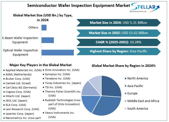
The Semiconductor Wafer Inspection Equipment Market size was valued at USD 5.31 Bn. in 2024 and the total Semiconductor Wafer Inspection Equipment Market revenue is expected to grow at a CAGR of 10.28 % from 2025 to 2032, reaching nearly USD 11.62 Bn. by 2032.
Semiconductor Wafer Inspection Equipment Market Overview
The Semiconductor Wafer Inspection Equipment Market plays a pivotal role in ensuring the quality and reliability of semiconductor devices. This equipment is essential for detecting and analyzing defects on semiconductor wafers, enabling manufacturers to maintain high production standards and yield rates. The market for semiconductor wafer inspection equipment has been experiencing steady growth in recent years, driven by the increasing demand for advanced semiconductor technologies across various industries. As semiconductor devices continue to evolve and become more complex, the need for reliable wafer inspection equipment is expected to further fuel the growth of this market. Industry experts and market research suggest a promising outlook for the Semiconductor Wafer Inspection Equipment Market, with continued expansion and technological advancements anticipated in the coming years.
To get more Insights: Request Free Sample Report
The growing demand for semiconductors has led to a significant rise in the need for automation systems to detect production flaws, driving growth in the Semiconductor Wafer Inspection Equipment Market. For instance, in January 2023, Innodisk Corporation, a prominent supplier of industrial embedded flash and storage products & technologies based in Taiwan, announced the development of DDR5 series DRAM designed to power semiconductor autonomous optical inspection. Automated optical inspection (AOI) applications, which address issues related to consumer-grade dynamic random-access memory (DRAM), are now essential at every stage of the semiconductor production process. These AOI solutions rely heavily on DDR5 series DRAM, further emphasizing the critical role of advanced technology in the Semiconductor Wafer Inspection Equipment Market.
Semiconductor Wafer Inspection Equipment Market Dynamics:
The Semiconductor Wafer Inspection Equipment Market is witnessing a surge in demand driven by the need for high-performance semiconductor materials propelled by various sectors such as smartphones, consumer electronics, automotive, and emerging technologies like 5G and AI. With the advent of the Internet of Things (IoT), there's a growing trend towards intelligent products, prompting the semiconductor industry to invest in advanced inspection equipment. This demand is further bolstered by the increasing need for metrology equipment to meet the rising demand for electronic goods. Technological advancements have enabled the development of next-generation, highly precise equipment with active process control systems, facilitating steady semiconductor wafer inspection equipment market growth.
Furthermore, the proliferation of connected devices globally, coupled with the importance of metrology in semiconductor development, highlights the necessity for accurate inspection tools to maintain low error rates and extend device lifespans. Despite these promising trends, the market faces challenges such as the high cost of equipment, which could limit accessibility for smaller manufacturers or those with constrained budgets. Additionally, environmental concerns surrounding the manufacturing processes of these tools pose a threat, necessitating investments in eco-friendly practices to mitigate operational costs, ensure regulatory compliance, and sustain semiconductor wafer inspection equipment market growth. Despite these challenges, the Semiconductor Wafer Inspection Equipment industry is poised for significant opportunities during the forecast period.
Analysing KLA Corporation's Impact on the Semiconductor Wafer Inspection Market:
The Semiconductor Wafer Inspection Equipment Market is prominently influenced by industry leaders like KLA Corporation, an American capital equipment company specializing in supplying process control and yield management systems for the semiconductor industry and other nanoelectronics sectors.

KLA Corporation's significant presence in the market is underscored by its substantial total revenue, which amounted to approximately 10.5 billion U.S. dollars in 2023. Notably, within this revenue stream, wafer inspection stands out as the primary contributor, accounting for about 4.34 billion U.S. dollars in 2023. This substantial contribution underscores the pivotal role of wafer inspection equipment in the semiconductor industry, reflecting its critical importance in ensuring quality control and yield optimization throughout the manufacturing process. KLA Corporation's dominance in this segment highlights its technological prowess and market leadership, solidifying its position as a key player shaping the trajectory of the semiconductor wafer inspection equipment market.
Semiconductor Wafer Inspection Equipment Market Segment Analysis
Based on Type, Optical Wafer Inspection Equipment segment dominated the market in 2024 and is expected to hold the largest Semiconductor Wafer Inspection Equipment Market share over the forecast period. Optical wafer inspection technology stands as the predominant choice within the semiconductor manufacturing industry. This method conducts thorough wafer inspections by analyzing the wavelength of light reflected from both patterned and un-patterned areas on the wafer. It is typically categorized into two main types: Brightfield inspection, utilizing light sources with a wavelength of 193 nm. Over time, advancements in technology have significantly enhanced the sensitivity of optical wafer inspection equipment.
Consequently, optical wafer inspection has become the preferred method across various semiconductor manufacturing facilities, including foundries and IDMs. As the number of semiconductors fabs continues to rise, the demand for optical wafer inspection equipment is poised to follow suit, thereby driving semiconductor wafer inspection equipment market growth significantly within the optical wafer inspection segment throughout the forecast period.
By End-user, The Foundries segment generated the highest revenue in 2024. Mobile devices, set-top boxes, network switches, smartphones, tablets, notebooks, gaming consoles, and digital cameras represent just a sampling of the diverse range of products driving this demand. As consumer preferences continue to evolve, with an increasing reliance on digital connectivity and technological innovations, foundries stand at the forefront of meeting these demands. Their role in the production of semiconductors for a wide array of electronic applications positions them as key players in the Semiconductor Wafer Inspection Equipment Market. Moreover, as technological advancements spur the development of more sophisticated devices and the proliferation of IoT-connected gadgets, the significance of foundries in driving semiconductor wafer inspection equipment market growth is expected to further amplify in the coming years.
Semiconductor Wafer Inspection Equipment Market Regional Insight:
Asia-Pacific hold largest market share of nearly 42% in 2024. Renowned for its pivotal role in both semiconductor production and consumption, Asia-Pacific stands as a critical region within the semiconductor industry landscape. China commands the largest share of the Asia-Pacific semiconductor market, a testament to its significant influence in the sector, as asserted by the Semiconductor Industry Association (SIA). Semiconductor wafer inspection equipment market is witnessing a surge in collaboration and partnership agreements among local businesses, indicative of the region's commitment to fostering a robust, self-sufficient semiconductor ecosystem. Notably, examples include the landmark five-year memorandum of understanding between Huawei's HiSilicon Technologies and Shenzhen JT Automation Equipment, aimed at bolstering semiconductor packaging tool development and enhancing industry regulation.
North America is poised to experience steady growth at a CAGR of 11.05%, generating USD XX billion throughout the forecast period. The semiconductor industry in the United States and Canada maintains global leadership in cutting-edge technologies such as 5G, quantum computing, and artificial intelligence (AI). Despite encountering negative year-over-year sales growth in 2019, the American semiconductor sector has consistently commanded a significant share of the worldwide semiconductor wafer inspection equipment market, sustaining substantial investments in Research and Development (R&D) and capital expenditures. Particularly, a considerable portion of these investments is directed towards supporting advanced fabrication facilities across the US, where 18 states host semiconductor fab capacity, thus bolstering exports and employment opportunities.
European region holds a smaller market share than APAC due to the limited presence of semiconductor manufacturing companies. However, significant investments in aerospace, defense, automotive, and renewable energy sectors are anticipated to significantly impact semiconductor demand over the forecast period. The increasing consumer demand for electronic devices further fuels the region's semiconductor wafer inspection equipment market, driving year-over-year growth. Moreover, efforts towards vertical integration and consolidation within the European fabrication sector have bolstered the capacity of semiconductor firms to invest in growth initiatives. These transformative market dynamics are expected to fuel demand for new semiconductor fabrication and processing facilities, thereby amplifying the necessity for semiconductor metrology and inspection tools.
Semiconductor Wafer Inspection Equipment Market Country-wise Analysis:
The Semiconductor Wafer Inspection Equipment Market demonstrates diverse dynamics across various countries, with notable trends and developments shaping each region's landscape. In China, a powerhouse in semiconductor manufacturing, the demand for wafer inspection equipment is sustained by the country's burgeoning electronics industry and government-backed initiatives to bolster semiconductor production. Similarly, the United States, with its strong emphasis on technological innovation and leadership in AI, 5G, and IoT, drives significant demand for high-performance semiconductor materials and advanced inspection tools.
South Korea, home to major semiconductor giants like Samsung and SK Hynix, stands as another pivotal semiconductor wafer inspection equipment market cision-oriented manufacturing practices, fosters demand for top-tier wafer inspection equipment, especially in automotive electronics and industrial automation. Taiwan's semiconductor industry, led by companies like TSMC, fuels demand for cutting-edge inspection solutions to support its position in semiconductor fabrication technologies.
Germany's semiconductor sector benefits from its focus on automotive and industrial technology, necessitating sophisticated wafer inspection equipment to maintain stringent quality standards. Singapore's strategic positioning and conducive business environment drive demand for wafer inspection equipment, supporting its semiconductor manufacturing and research endeavors. While these countries represent key hubs in the Semiconductor Wafer Inspection Equipment Market, emerging semiconductor industries in countries like India, Malaysia, and Vietnam also contribute to the global market's growth trajectory, albeit to varying degrees.
Industrial News:
In the Semiconductor Wafer Inspection Equipment Market, significant industrial developments have been observed for examples:
- July 2023: Applied Materials Inc. unveiled cutting-edge materials, technologies, and systems designed to facilitate the seamless integration of chiplets into advanced 2.5D and 3D packages using hybrid bonding and through-silicon vias (TSVs). These innovative solutions represent an expansion of the company's extensive range of technologies tailored for heterogeneous integration (HI), reinforcing its position as a leading supplier in this field. Applied Materials Inc. offers a comprehensive suite of optimized chipmaking systems, covering etch, physical and chemical vapor deposition (PVD), electroplating, chemical mechanical polishing (CMP), annealing, and surface treatments. This empowers chipmakers with the tools necessary to advance their HI initiatives effectively.
- December 2022: Applied Materials, Inc. introduced two new cold field emission (CFE) e-beam products – SEMVision G10 for defect review and PrimeVision 10 for defect identification. This move aims to maintain the company's dominant position in the e-beam process diagnostics & control space, showcasing its commitment to innovation and leadership in the semiconductor industry.
Global Semiconductor Wafer Inspection Equipment Market Scope:
|
Semiconductor Wafer Inspection Equipment Market |
|
|
Market Size in 2024 |
USD 5.31 Bn. |
|
Market Size in 2032 |
USD 11.62 Bn. |
|
CAGR (2025-2032) |
10.28% |
|
Historic Data |
2019-2024 |
|
Base Year |
2024 |
|
Forecast Period |
2025-2032 |
|
Segments |
By Type Optical Wafer Inspection Equipment E-Beam Wafer Inspection Equipment Others |
|
|
By End-user Foundries IDMs |
|
Regional Scope |
North America- United States, Canada, and Mexico Europe – UK, France, Germany, Italy, Spain, Sweden, Russia, and Rest of Europe Asia Pacific – China, India, Japan, South Korea, Australia, ASEAN, Rest of APAC Middle East and Africa - South Africa, GCC, Egypt, Nigeria, Rest of the Middle East and Africa South America – Brazil, Argentina, Rest of South America |
Leading Semiconductor Wafer Inspection Equipment manufacturers include
- Applied Materials Inc. (USA)
- ASML (Netherlands)
- Bruker Corp. (USA)
- Camtek Ltd. (Israel)
- Carl Zeiss AG (Germany)
- Cognex Corp. (USA)
- Hitachi Ltd. (Japan)
- JEOL Ltd. (Japan)
- KLA Corp. (USA)
- Lam Research Corp. (USA)
- Lasertec Corp. (Japan)
- Nanometrics Inc. (now part of Onto Innovation) (USA)
- Nikon Corp. (Japan)
- Nova Measuring Instruments Ltd. (Israel)
- NXP Semiconductors NV (Netherlands)
- Onto Innovation Inc. (USA)
- Synopsys Inc. (USA)
- Teradyne Inc. (USA)
- Toray Industries Inc. (Japan)
- TSI Inc. (USA)
- Thermo Fisher Scientific Inc. (USA)
- Rudolph Technologies (now part of Onto Innovation) (USA)
- Veeco Instruments Inc. (USA)
- FEI Company (now part of Thermo Fisher Scientific) (USA)
- Tokyo Electron Ltd. (TEL) (Japan)
Frequently Asked Questions
Semiconductor wafer inspection equipment is commonly used for defect detection, dimensional analysis, wafer mapping, overlay alignment, thin film and material analysis, and electrical characterization in semiconductor manufacturing processes.
The growth of the Semiconductor Wafer Inspection Equipment market is driven by increasing demand for high-performance semiconductor materials, technological advancements, and investment in metrology equipment to meet the growing demand for electronic goods.
The market is segmented into Optical Wafer Inspection Equipment, E-Beam Wafer Inspection Equipment and Others type.
The Asia-Pacific region is experiencing the fastest growth in the Semiconductor Wafer Inspection Equipment market, driven by its prominent semiconductor manufacturing hubs and increasing demand for electronic devices, followed by North America and Europe.
1. Semiconductor Wafer Inspection Equipment Market: Research Methodology
1.1. Research Data
1.1.1. Primary Data
1.1.2. Secondary Data
1.2. Market Size Estimation
1.2.1. Bottom-Up Approach
1.2.2. Top-Down Approach
1.3. Market breakdown and Data Triangulation
1.4. Assumptions
2. Semiconductor Wafer Inspection Equipment Market: Executive Summary
2.1. Market Overview
2.2. Market Size (2024) and Forecast (2025– 2032) and Y-O-Y%
2.3. Market Size (USD) and Market Share (%) – By Segments and Regions
3. Semiconductor Wafer Inspection Equipment Market: Competitive Landscape
3.1. Stellar Competition Matrix
3.2. Key Players Benchmarking
3.2.1. Company Name
3.2.2. Headquarter
3.2.3. Product Segment
3.2.4. End-user Segment
3.2.5. Y-O-Y%
3.2.6. Revenue (2024)
3.2.7. Profit Margin
3.2.8. Market Share
3.2.9. Company Locations
3.3. Market Structure
3.3.1. Market Leaders
3.3.2. Market Followers
3.3.3. Emerging Players
3.4. Consolidation of the Market
3.4.1. Strategic Initiatives and Developments
3.4.2. Mergers and Acquisitions
3.4.3. Collaborations and Partnerships
3.4.4. Product Launches and Innovation
4. Semiconductor Wafer Inspection Equipment Market: Dynamics
4.1. Market Trends by Region
4.1.1. North America
4.1.2. Europe
4.1.3. Asia Pacific
4.1.4. Middle East and Africa
4.1.5. South America
4.2. Market Drivers
4.3. Market Restraints
4.4. Market Opportunities
4.5. Market Challenges
4.6. PORTER’s Five Forces Analysis
4.6.1. Intensity of the Rivalry
4.6.2. Threat of New Entrants
4.6.3. Bargaining Power of Suppliers
4.6.4. Bargaining Power of Buyers
4.6.5. Threat of Substitutes
4.7. PESTLE Analysis
4.7.1. Political Factors
4.7.2. Economic Factors
4.7.3. Social Factors
4.7.4. Technological Factors
4.7.5. Legal Factors
4.7.6. Environmental Factors
4.8. Technological Roadmap
4.9. Value Chain Analysis
4.10. Regulatory Landscape by Region
4.10.1. North America
4.10.2. Europe
4.10.3. Asia Pacific
4.10.4. Middle East and Africa
4.10.5. South America
5. Semiconductor Wafer Inspection Equipment Market Size and Forecast by Segments (by Value USD Million)
5.1. Semiconductor Wafer Inspection Equipment Market Size and Forecast, By Type (2024-2032)
5.1.1. Optical Wafer Inspection Equipment
5.1.2. E-Beam Wafer Inspection Equipment
5.1.3. Others
5.2. Semiconductor Wafer Inspection Equipment Market Size and Forecast, By End-user (2024-2032)
5.2.1. Foundries
5.2.2. IDMs
5.3. Semiconductor Wafer Inspection Equipment Market Size and Forecast, by Region (2024-2032)
5.3.1. North America
5.3.2. Europe
5.3.3. Asia Pacific
5.3.4. Middle East and Africa
5.3.5. South America
6. North America Semiconductor Wafer Inspection Equipment Market Size and Forecast (by Value USD Million)
6.1. North America Semiconductor Wafer Inspection Equipment Market Size and Forecast, By Type (2024-2032)
6.1.1. Optical Wafer Inspection Equipment
6.1.2. E-Beam Wafer Inspection Equipment
6.1.3. Others
6.2. North America Semiconductor Wafer Inspection Equipment Market Size and Forecast, By End-user (2024-2032)
6.2.1. Foundries
6.2.2. IDMs
6.3. North America Semiconductor Wafer Inspection Equipment Market Size and Forecast, by Country (2024-2032)
6.3.1. United States
6.3.2. Canada
6.3.3. Mexico
7. Europe Semiconductor Wafer Inspection Equipment Market Size and Forecast (by Value USD Million)
7.1. Europe Semiconductor Wafer Inspection Equipment Market Size and Forecast, By Type (2024-2032)
7.2. Europe Semiconductor Wafer Inspection Equipment Market Size and Forecast, By End-user (2024-2032)
7.3. Europe Semiconductor Wafer Inspection Equipment Market Size and Forecast, by Country (2024-2032)
7.3.1. UK
7.3.2. France
7.3.3. Germany
7.3.4. Italy
7.3.5. Spain
7.3.6. Sweden
7.3.7. Austria
7.3.8. Rest of Europe
8. Asia Pacific Semiconductor Wafer Inspection Equipment Market Size and Forecast (by Value USD Million)
8.1. Asia Pacific Semiconductor Wafer Inspection Equipment Market Size and Forecast, By Type (2024-2032)
8.2. Asia Pacific Semiconductor Wafer Inspection Equipment Market Size and Forecast, By End-user (2024-2032)
8.3. Asia Pacific Semiconductor Wafer Inspection Equipment Market Size and Forecast, by Country (2024-2032)
8.3.1. China
8.3.2. S Korea
8.3.3. Japan
8.3.4. India
8.3.5. Australia
8.3.6. Indonesia
8.3.7. Malaysia
8.3.8. Vietnam
8.3.9. Taiwan
8.3.10. Bangladesh
8.3.11. Pakistan
8.3.12. Rest of Asia Pacific
9. Middle East and Africa Semiconductor Wafer Inspection Equipment Market Size and Forecast (by Value USD Million)
9.1. Middle East and Africa Semiconductor Wafer Inspection Equipment Market Size and Forecast, By Type (2024-2032)
9.2. Middle East and Africa Semiconductor Wafer Inspection Equipment Market Size and Forecast, By End-user (2024-2032)
9.3. Middle East and Africa Semiconductor Wafer Inspection Equipment Market Size and Forecast, by Country (2024-2032)
9.3.1. South Africa
9.3.2. GCC
9.3.3. Egypt
9.3.4. Nigeria
9.3.5. Rest of ME&A
10. South America Semiconductor Wafer Inspection Equipment Market Size and Forecast (by Value USD Million)
10.1. South America Semiconductor Wafer Inspection Equipment Market Size and Forecast, By Type (2024-2032)
10.2. South America Semiconductor Wafer Inspection Equipment Market Size and Forecast, By End-user (2024-2032)
10.3. South America Semiconductor Wafer Inspection Equipment Market Size and Forecast, by Country (2024-2032)
10.3.1. Brazil
10.3.2. Argentina
10.3.3. Rest of South America
11. Company Profile: Key players
11.1. Applied Materials Inc. (USA)?
11.1.1. Company Overview
11.1.2. Product Portfolio
11.1.2.1. Product Name
11.1.2.2. Product Details
11.1.3. Financial Overview
11.1.3.1. Total Revenue
11.1.3.2. Segment Revenue
11.1.3.3. Regional Revenue
11.1.4. SWOT Analysis
11.1.5. Strategic Analysis
11.1.6. Recent Developments
11.2. ASML (Netherlands)?
11.3. Bruker Corp. (USA)
11.4. Camtek Ltd. (Israel)?
11.5. Carl Zeiss AG (Germany)
11.6. Cognex Corp. (USA)
11.7. Hitachi Ltd. (Japan)? ?
11.8. JEOL Ltd. (Japan)?
11.9. KLA Corp. (USA)?
11.10. Lam Research Corp. (USA)
11.11. Lasertec Corp. (Japan)?
11.12. Nanometrics Inc. (now part of Onto Innovation) (USA)
11.13. Nikon Corp. (Japan)?
11.14. Nova Measuring Instruments Ltd. (Israel)?
11.15. NXP Semiconductors NV (Netherlands)
11.16. Onto Innovation Inc. (USA)?
11.17. Synopsys Inc. (USA)
11.18. Teradyne Inc. (USA)
11.19. Toray Industries Inc. (Japan)
11.20. TSI Inc. (USA)
11.21. Thermo Fisher Scientific Inc. (USA)?
11.22. Rudolph Technologies (now part of Onto Innovation) (USA)
11.23. Veeco Instruments Inc. (USA)
11.24. FEI Company (now part of Thermo Fisher Scientific) (USA)
11.25. Tokyo Electron Ltd. (TEL) (Japan)
12. Key Findings
13. Industry Recommendations
13.1. Strategic Recommendations
13.2. Future Outlook