Semiconductor Bonding Market Industry Analysis and Forecast (2026-2032) Trends, Statistics, Dynamics, Segmentation
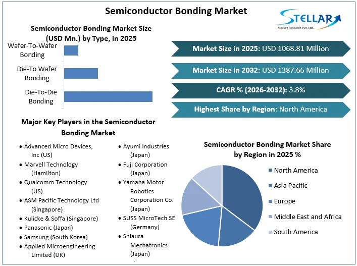
Semiconductor Bonding Market is predicted to grow at a CAGR of 3.8% during the forecast period. The Global Semiconductor Bonding Market is expected to reach US$ 1387.66 Mn. in 2032 from US$ 1068.81 Mn in 2025.
Semiconductor Bonding Market Overview
Semiconductor bonding is used to create composite 3D structures, cavities, and closed fluid channels that are both mechanically and electrically strong. It is critical to firmly connect two or more micro-components. Nanomaterials and microscopic computer systems are also created using semiconductor bonding.
The global semiconductor bonding market is rapidly expanding. Semiconductors can be found in a wide range of electronic devices. Semiconductor technology has enormous potential to transform industries such as healthcare, manufacturing, aerospace, and defense by providing a variety of innovative electronic devices. As a result, the market is receiving more funding and support from both public and private organizations. With significant investments from OEMs, venture capitalists, and government bodies, the market is predicted to grow at an exponential rate in the forecasted years.
To get more Insights: Request Free Sample Report
Semiconductor Bonding Market Dynamics
The market is expected to grow significantly as a result of rising demand for miniature electronic components, increased adoption of stacked die technology in IoT devices, and rising demand for electric and hybrid vehicles. The high ownership cost is expected to stifle market growth. However, rising demand for 3D semiconductor assembly and packaging, as well as the growing adoption of IoT and AI in the automotive industry, present an opportunity for semiconductor bonding vendors.
The complex manufacturing processes of semiconductor bonding designs, as well as the constantly changing semiconductor industry, are major factors impeding the market growth. Furthermore, the high production costs of semiconductor bonding pose significant barriers to market growth. Nonetheless, the increasing use of semiconductor bonding in power switching applications would support market growth throughout the forecasted period.
Market Drivers
- The growing use of stacked die technology in IoT devices is propelling the semiconductor bonding market towards growth. Stacked die refers to the process of stacking one die on top of another within a single semiconductor package. Die stacking improves electrical device performance because shorter interconnection routing between circuits results in faster signal transmission.
- In the semiconductor industry, original equipment manufacturers (OEMs) are focusing on leveraging the benefits of IoT beyond connectivity. Sensors, RFID tags, smart meters, smart beacons, and distribution control systems are among the IoT devices and technologies that are increasingly being used in applications such as buildings and home automation, connected logistics, smart retail, smart mobility, and transportation, etc.
- Further, the increasing use of semiconductor platforms in healthcare, automotive & aerospace, defense, and consumer electronics boosts market value. Increased applications in voice recognition, machine vision (ML), and video monitoring have an impact on market growth.
Market Restraints
- Semiconductor bonding equipment is complex machinery that requires a lot of power to perform die attach operations. The amount of power used by this equipment ranges from hundreds to thousands of watts.
- The manufacturing costs of semiconductor bonding equipment are also high due to the use of complex, expensive components, and the assembly of various big and small parts, such as the screen, bonding hand, vacuum, sensors, and heat source, is also expensive. As a result, the overall production and ownership costs of die bonder equipment for semiconductor bonding are relatively high.
- The exorbitant cost of semiconductor wafers increases the operating cost of the semiconductor bonding, thereby hindering the market's growth.
- Due to the high cost and difficulty of designing semiconductor chips at the most advanced nodes, many chipmakers are beginning to split that chip into several sections, not all of which require leading-edge nodes. When a complex system is integrated monolithically on a single piece of silicon, the end result is a compromise between the thermal budget constraints of a device's component.
Market Opportunities
- Growing demand for miniatures of electronics products and portable devices creates several market opportunities; at the same time, the rising use of various electronic devices such as smartphones, computers, and military weapons, among others, creates significant market opportunities.
- The growing demand for thin wafers in the semiconductor industry is a major driver of the wafer bonding market's expansion.
- Increased production capacity is predicted to meet the growing demand for high-quality silicon wafers. Such expansions are driving up demand for wafer bonding equipment.
Market Challenges
- Mechanical movements are used by die bonder equipment to pick and place the die for the bonding process. Many moving parts in the equipment necessitate precise movement in order to accurately attach the die to the substrate. Mechanical part vibration has become a major challenge for semiconductor bonding equipment manufacturers, which must be overcome.
- Thin wafer is brittle and easily damaged by pressure or stress. A thin wafer is highly flexible and can break even under light pressure or stress. Die made from thin wafers can easily break during the internal wafer thinning process.
Semiconductor Bonding Market Regional Insights
By Region, the global semiconductor bonding market is categorized into North America, Europe, Asia-Pacific, the Middle East & Africa, and South America.
North America - The continued innovation, primarily in the IT, telecom, and automotive industries, has driven the growth of the North American electronic manufacturing and design services market. Strategic collaborations aimed at instilling sophisticated technologies and advancing existing technologies are also predicted to drive growth in the North American semiconductor bonding market during the forecast period.
Europe - The increasing adoption of modern technologies, as well as the growing number of small and medium-sized businesses, are expected to drive the growth of the European semiconductor bonding market (SMEs). Rising technological adoption, a focus on innovations derived from R&D and Technology, more IT organizations, and ongoing projects will drive the European market forward.
Asia Pacific - Due to the faster adoption of advanced technologies in the Region's developing countries—China, Japan, and India—Asia-Pacific is expected to be the dominant regional market. As Asia-technological Pacific's awareness grows, so does the market for consumer electronics. Similarly, mass production of electronic products such as smartphones, wearables, and white goods in China and Taiwan is expected to accelerate market growth in Asia Pacific.
South America and The Middle East & Africa - These regions grow at a comparatively low pace as other regions. -
Semiconductor Bonding Market Segment Analysis
The global semiconductor bonding market is segmented based on process type, Technology, and Application.
By process type, the market is segmented into Die-To-Die Bonding, Die-To Wafer Bonding, and Wafer-To-Wafer Bonding.
In 2025, the wafer bonder segment dominated the market with a market share of approximately 41.2 percent. Wafer bonding is increasingly being used in silicon-on-insulator (SOI) devices, silicon-based sensors and actuators, and optical devices. Wafer bonding technology provides numerous benefits, including the prevention of surface bubbles, the bonding of various compounds, low-temperature bonding, high vacuum bonding, and a thinning method for the smart cut procedure. Wafer bonding allows for greater design and fabrication freedom in material combinations, which is undoubtedly a major factor in the global growth of the Semiconductor bonding market.
By Technology, the market is segmented into Die Bonding Technology (Flip-chip Attachment, Epoxy Die Bonding, Hybrid Bonding, and Eutectic Die Bonding) and Wafer Bonding Technology (TCB Wafer Bonding, Direct Wafer Bonding, Hybrid Bonding, and Anodic Wafer Bonding).
The Die Bonding segment dominated the market in 2025, accounting for approximately 64.2 percent of market share. Die bonding is a semiconductor wrapping production method. It is the process of attaching a die (or chip) to a material or package using adhesive or sinter, also referred to as die to attach or die placement. The process starts with selecting a die from a waffle pack and placing it on the material. The die is inserted into previously applied epoxy.
Based on Application, the market has been segmented into RF Devices, MEMS and Sensors, CMOS Image Sensors, LED, and 3D NAND.

Even globally, the LED is anticipated to be the fastest-growing application segment of the semiconductor bonding market, with a CAGR of 5% between 2026 and 2032. Due to the growing penetration of LEDs in several sectors, such as consumer electronics, automotive, commercial, residential, and architectural, this segment has had a lower impact than other segments. LED lighting is widely used in commercial and industrial settings because of its numerous advantages, including energy efficiency, reduced heat emissions, cost-effectiveness, and nanosecond switching capability. Thin wafers are used in LED devices for a variety of reasons, including high efficiency and low power consumption.
The purpose of this report is to provide stakeholders in the industry with a comprehensive analysis of the global semiconductor bonding market. The report discusses the most important trends in the global semiconductor bonding market, as well as how these trends will affect new business investments and market growth over the forecast period. The report also analyses market leaders, market followers, and regional players to help understand the Global Semiconductor Bonding Market dynamics and competitive structure.
The qualitative and quantitative data in the Global Semiconductor Bonding Market report is aimed to aid in determining which market segments, regions, and factors affecting the market are expected to grow at higher rates, as well as key opportunity areas that will drive the industry and market growth over the forecast period. The competitive landscape of key industry players, as well as their recent developments in the Global Semiconductor Bonding Market, is also included in the report. The report looks at things like company size, market share, market growth, revenue, production volume, and profits for the major players in the global semiconductor bonding market.
The report provides Porter's Five Force Model, which helps in designing the business strategies in the market. The report helps in identifying how many rivals exist, who they are, and how their product quality is in the Global Semiconductor bonding market. The report also analyses if the Global Semiconductor bonding market is easy for a new player to gain a foothold in the market, do they enter or exit the market regularly, if the market is dominated by a few players, etc.
A PESTEL Analysis is also included in the report, which aids in the development of company strategies. Political variables assist in determining the extent to which a government can influence the global semiconductor bonding market. Economic variables are useful for analyzing economic performance drivers that affect the global semiconductor bonding market. Legal factor aids in understanding the impact of the surrounding environment and the impact of environmental concerns on the global semiconductor bonding market.
Semiconductor Bonding Market Scope
|
Semiconductor Bonding Market |
|
|
Market Size in 2025 |
USD 1068.81 Mn. |
|
Market Size in 2032 |
USD 1387.66 Mn. |
|
CAGR (2026-2032) |
3.8% |
|
Historic Data |
2020-2025 |
|
Base Year |
2025 |
|
Forecast Period |
2026-2032 |
|
Segment Scope |
by Type
|
|
by Technology
|
|
|
By Application
|
|
|
Regional Scope |
North America- United States, Canada, and Mexico Europe – UK, France, Germany, Italy, Spain, Sweden, Austria, and Rest of Europe Asia Pacific – China, India, Japan, South Korea, Australia, ASEAN, Rest of APAC Middle East and Africa - South Africa, GCC, Egypt, Nigeria, Rest of the Middle East and Africa South America – Brazil, Argentina, Rest of South America |
Semiconductor Bonding Market Key Players
- Advanced Micro Devices, Inc (US)
- Marvell Technology (Hamilton)
- Qualcomm Technology (US).
- ASM Pacific Technology Ltd (Singapore)
- Kulicke & Soffa (Singapore)
- Panasonic (Japan)
- Samsung (South Korea)
- Applied Microengineering Limited (UK)
- ASM Pacific Technology (Singapore)
- Ayumi Industries (Japan)
- Fuji Corporation (Japan)
- Yamaha Motor Robotics Corporation Co. (Japan)
- SUSS MicroTech SE (Germany)
- Shiaura Mechatronics (Japan)
- Intel Corporation (US)
- Google. Inc (US)
- NVIDIA Corporation (US)
- Xilinx Inc. (US)
- IBM Corporation (US)
Frequently Asked Questions
The Semiconductor Bonding Market is estimated to grow at a rate of 3.8% CAGR in the forecasted period (2026-2032).
The Global Semiconductor Bonding Market is expected to reach US$ 1387.66 Mn. in 2032 from US$ 1068.81 Mn in 2025.
Some of the key players are Advanced Micro Devices, Inc (US), Marvell Technology (Hamilton), Qualcomm Technology (US), ASM Pacific Technology Ltd (Singapore), Kulicke & Soffa (Singapore), Panasonic (Japan), Fuji Corporation (Japan), Yamaha Motor Robotics Corporation Co. (Japan)
1. Semiconductor Bonding Market: Research Methodology
1.1. Research Data
1.1.1. Primary Data
1.1.2. Secondary Data
1.2. Market Size Estimation
1.2.1. Bottom-Up Approach
1.2.2. Top-Down Approach
1.3. Market breakdown and Data Triangulation
1.4. Assumptions
2. Semiconductor Bonding Market: Executive Summary
2.1. Market Overview
2.2. Market Size (2025) and Forecast (2026 – 2032) and Y-O-Y%
2.3. Market Size (USD) and Market Share (%) – By Segments and Regions
3. Semiconductor Bonding Market: Competitive Landscape
3.1. Stellar Competition Matrix
3.2. Key Players Benchmarking
3.2.1. Company Name
3.2.2. Headquarter
3.2.3. Business Segment
3.2.4. End-user Segment
3.2.5. Y-O-Y%
3.2.6. Revenue (2025)
3.2.7. Profit Margin
3.2.8. Market Share
3.2.9. Company Locations
3.3. Market Structure
3.3.1. Market Leaders
3.3.2. Market Followers
3.3.3. Emerging Players
3.4. Consolidation of the Market
3.4.1. Strategic Initiatives and Developments
3.4.2. Mergers and Acquisitions
3.4.3. Collaborations and Partnerships
3.4.4. Product Launches and Innovations
4. Semiconductor Bonding Market: Dynamics
4.1. Market Trends by Region
4.1.1. North America
4.1.2. Europe
4.1.3. Asia Pacific
4.1.4. Middle East and Africa
4.1.5. South America
4.2. Market Drivers
4.3. Market Restraints
4.4. Market Opportunities
4.5. Market Challenges
4.6. PORTER’s Five Forces Analysis
4.6.1. Intensity of the Rivalry
4.6.2. Threat of New Entrants
4.6.3. Bargaining Power of Suppliers
4.6.4. Bargaining Power of Buyers
4.6.5. Threat of Substitutes
4.7. PESTLE Analysis
4.7.1. Political Factors
4.7.2. Economic Factors
4.7.3. Social Factors
4.7.4. Technological Factors
4.7.5. Legal Factors
4.7.6. Environmental Factors
4.8. Technological Roadmap
4.9. Regulatory Landscape
4.9.1. Market Regulation by Region
4.9.1.1. North America
4.9.1.2. Europe
4.9.1.3. Asia Pacific
4.9.1.4. Middle East and Africa
4.9.1.5. South America
4.9.2. Impact of Regulations on Market Dynamics
4.9.3. Government Schemes and Initiatives
5. Semiconductor Bonding Market Size and Forecast by Segments (by Value USD Million)
5.1. Semiconductor Bonding Market Size and Forecast, By Type (2025-2032)
5.1.1. Die-to-Die Bonding
5.1.2. Die-to Wafer Bonding
5.1.3. Wafer-to-Wafer Bonding
5.2. Semiconductor Bonding Market Size and Forecast, By Technology (2025-2032)
5.2.1. Die Bonding Technology
5.2.2. Wafer Bonding Technology
5.3. Semiconductor Bonding Market Size and Forecast, By Application (2025-2032)
5.3.1. RF Devices
5.3.2. MEMS and Sensors
5.3.3. CMOS Image Sensors
5.3.4. LED
5.3.5. 3D NAND
5.4. Semiconductor Bonding Market Size and Forecast, by Region (2025-2032)
5.4.1. North America
5.4.2. Europe
5.4.3. Asia Pacific
5.4.4. Middle East and Africa
5.4.5. South America
6. North America Semiconductor Bonding Market Size and Forecast (by Value USD Million)
6.1. North America Semiconductor Bonding Market Size and Forecast, By Type (2025-2032)
6.1.1. Die-to-Die Bonding
6.1.2. Die-to Wafer Bonding
6.1.3. Wafer-to-Wafer Bonding
6.2. North America Semiconductor Bonding Market Size and Forecast, By Technology (2025-2032)
6.2.1. Die Bonding Technology
6.2.2. Wafer Bonding Technology
6.3. North America Semiconductor Bonding Market Size and Forecast, By Application (2025-2032)
6.3.1. RF Devices
6.3.2. MEMS and Sensors
6.3.3. CMOS Image Sensors
6.3.4. LED
6.3.5. 3D NAND
6.4. North America Semiconductor Bonding Market Size and Forecast, by Country (2025-2032)
6.4.1. United States
6.4.2. Canada
6.4.3. Mexico
7. Europe Semiconductor Bonding Market Size and Forecast (by Value USD Million)
7.1. Europe Semiconductor Bonding Market Size and Forecast, By Type (2025-2032)
7.2. Europe Semiconductor Bonding Market Size and Forecast, By Technology (2025-2032)
7.3. Europe Semiconductor Bonding Market Size and Forecast, By Application (2025-2032)
7.4. Europe Semiconductor Bonding Market Size and Forecast, by Country (2025-2032)
7.4.1. UK
7.4.2. France
7.4.3. Germany
7.4.4. Italy
7.4.5. Spain
7.4.6. Sweden
7.4.7. Austria
7.4.8. Rest of Europe
8. Asia Pacific Semiconductor Bonding Market Size and Forecast (by Value USD Million)
8.1. Asia Pacific Semiconductor Bonding Market Size and Forecast, By Type (2025-2032)
8.2. Asia Pacific Semiconductor Bonding Market Size and Forecast, By Technology (2025-2032)
8.3. Asia Pacific Semiconductor Bonding Market Size and Forecast, By Application (2025-2032)
8.4. Asia Pacific Semiconductor Bonding Market Size and Forecast, by Country (2025-2032)
8.4.1. China
8.4.2. S Korea
8.4.3. Japan
8.4.4. India
8.4.5. Australia
8.4.6. Indonesia
8.4.7. Malaysia
8.4.8. Vietnam
8.4.9. Taiwan
8.4.10. Bangladesh
8.4.11. Pakistan
8.4.12. Rest of Asia Pacific
9. Middle East and Africa Semiconductor Bonding Market Size and Forecast (by Value USD Million)
9.1. Middle East and Africa Semiconductor Bonding Market Size and Forecast, By Type (2025-2032)
9.2. Middle East and Africa Semiconductor Bonding Market Size and Forecast, By Technology (2025-2032)
9.3. Middle East and Africa Semiconductor Bonding Market Size and Forecast, By Application (2025-2032)
9.4. Middle East and Africa Semiconductor Bonding Market Size and Forecast, by Country (2025-2032)
9.4.1. South Africa
9.4.2. GCC
9.4.3. Egypt
9.4.4. Nigeria
9.4.5. Rest of ME&A
10. South America Semiconductor Bonding Market Size and Forecast (by Value USD Million)
10.1. South America Semiconductor Bonding Market Size and Forecast, By Type (2025-2032)
10.2. South America Semiconductor Bonding Market Size and Forecast, By Technology (2025-2032)
10.3. South America Semiconductor Bonding Market Size and Forecast, By Application (2025-2032)
10.4. South America Semiconductor Bonding Market Size and Forecast, by Country (2025-2032)
10.4.1. Brazil
10.4.2. Argentina
10.4.3. Rest of South America
11. Company Profile: Key players
11.1. Advanced Micro Devices, Inc (US)
11.1.1. Overview
11.1.2. Business Portfolio
11.1.3. Financial Overview
11.1.3.1. Total Revenue
11.1.3.2. Segment Revenue
11.1.3.3. Regional Revenue
11.1.4. SWOT Analysis
11.1.5. Strategic Analysis
11.1.6. Recent Developments
11.2. Marvell Technology (Hamilton)
11.3. Qualcomm Technology (US).
11.4. ASM Pacific Technology Ltd (Singapore)
11.5. Kulicke & Soffa (Singapore)
11.6. Panasonic (Japan)
11.7. Samsung (South Korea)
11.8. Applied Microengineering Limited (UK)
11.9. ASM Pacific Technology (Singapore)
11.10. Ayumi Industries (Japan)
11.11. Fuji Corporation (Japan)
11.12. Yamaha Motor Robotics Corporation Co. (Japan)
11.13. SUSS MicroTech SE (Germany)
11.14. Shiaura Mechatronics (Japan)
11.15. Intel Corporation (US)
11.16. Google. Inc (US)
11.17. NVIDIA Corporation (US)
11.18. Xilinx Inc. (US)
11.19. IBM Corporation (US)
12. Key Findings
13. Industry Recommendations
13.1. Strategic Recommendations
13.2. Future Outlook